|
|
|
|
|
|
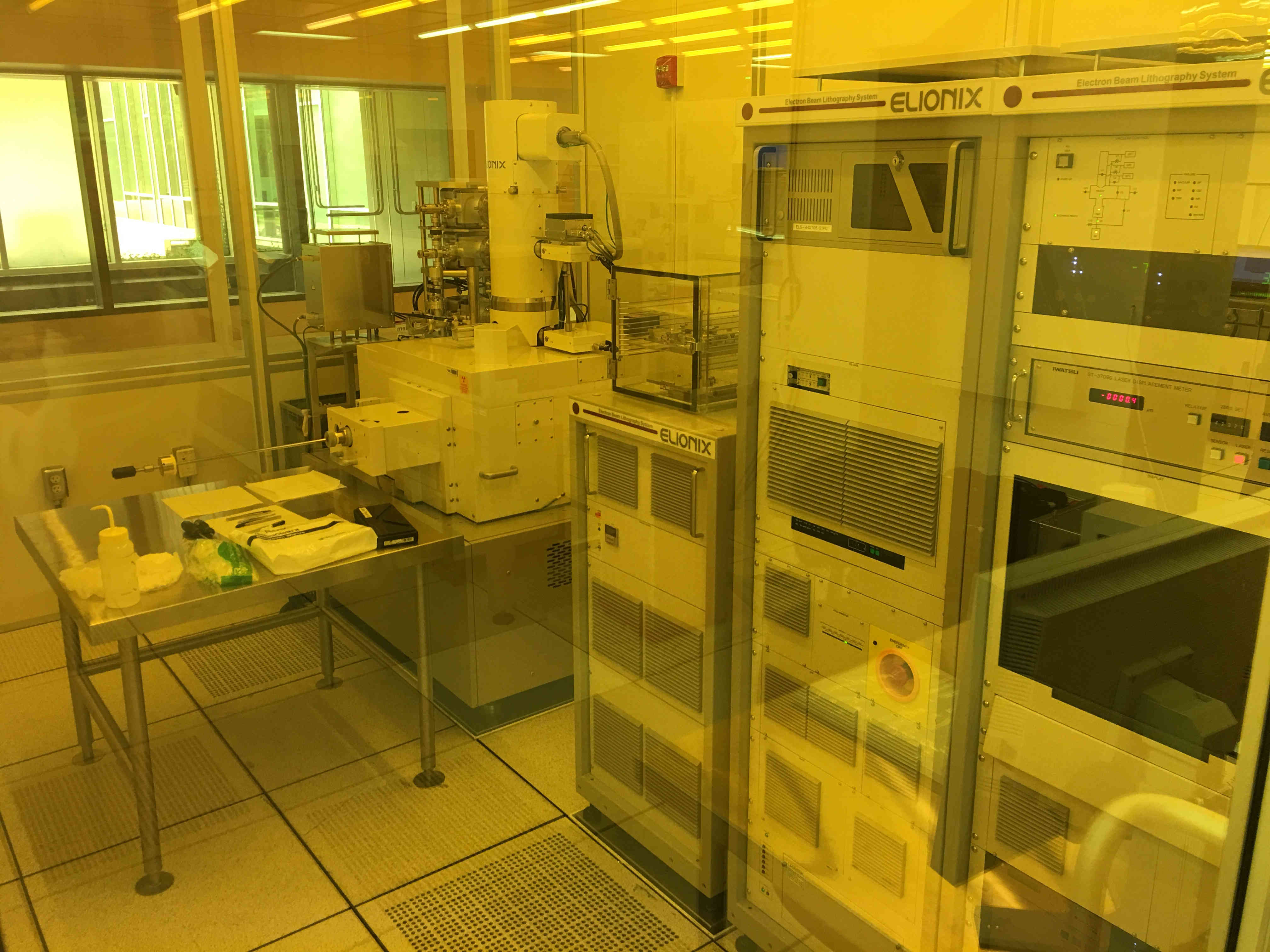
Electron Beam Lithography System:
Georgia Tech’s Institute for Electronics and Nanotechnology (IEN) currently operates an Elionix ELS-G100 100kV electron beam lithography system.
System Specifications:
- 1.8 nm diameter Gaussian spot electron beam
- 25, 50, or 100 kV acceleration
- 20 pA - 100 nA beam current
- 100 MHz scan speed
- maximum 1 mm field at 100 kV
- minimum pattern line width 6 nm
- 15 nm field stitching accuracy with 100 micron field
- 20 nm overlay (alignment) accuracy with 100 micron field
- ZrO/W thermal field emission
- maximum 8" diameter wafers down to millimeter size pieces
- can be used to make photomasks
- can be used for SEM imaging
|