|
|
|
|
|
|
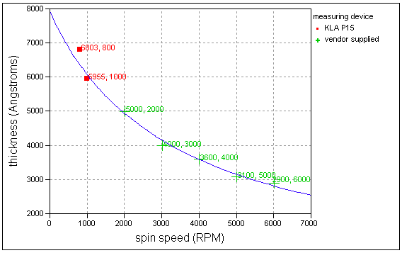
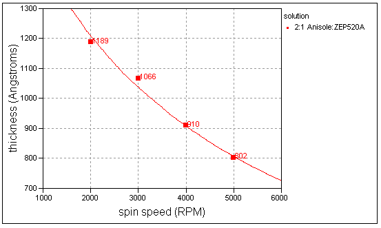
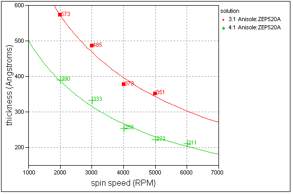
ZEP520A thickness vs. spin speed curves
undiluted ZEP520A
(1/y) = 1.259E-3 + (3.8E-8)x

Anisole:ZEP520A 1:1 dilution
3000 RPM, 1500RPM/s, 60sec on 4" wafer
mean = 1264 A, sigma = 11 A, N = 6
Anisole:ZEP520A 2:1 dilution
(1/y) = 5.48E-4 + (1.38E-7)x

Anisole:ZEP520A 3:1, 4:1 dilution
3:1 solution curve fit: (1/y) = 9.63E-4 + (3.88E-7)x
4:1 solution curve fit: (1/y) = 1.41E-3 + (5.82E-7)x

|


