|
|
|
|
|
|
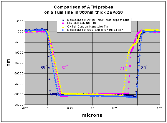
AFM is a useful technique, but tip selection is important for measuring lateral feature sizes when the aspect ratio of the feature is high. Tip selection must be carefully considered when performing AFM measurements of line measurements in resist.
Comparison of a MikroMasch NSC16 probe, Nanosensors AR10T-NCH high aspect ratio probe, CNTek Carbon Nanotube probe, and Nanosensors Super Sharp Silicon probe illustrating the impact to sidewall angle and linewidth measurement.
The line was drawn as 1um line surrounded by many 1um lines on both sides with 6um pitch.
The line was exposed with 200uC/cm2 dose, and developed in ZED-N50 for 2 minutes.
|