|
|
|
|
|
|
Nanoimprint templates can be made out of silicon by using electron beam lithography to a make a pattern in resist, and then transfer the pattern by plasma etching. Below is an example of an imprint template that was made with a 4" diameter silicon wafer. Because silicon is somewhat fragile (susceptible to cracking/cleaving), templates are sometimes made out of other materials such as nickel or quartz. Or sometimes, a silicon template is used as a master, and duplicate templates are made from the master.
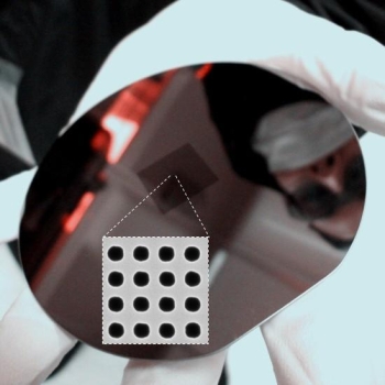
Shown in the above image is a 4" diameter crystalline silicon wafer with an array of 200 nm diameter holes on 300 nm pitch, etched to a depth of 500 nm and covering a 1.8 x 1.8 cm square area.
|